|
Research activities:
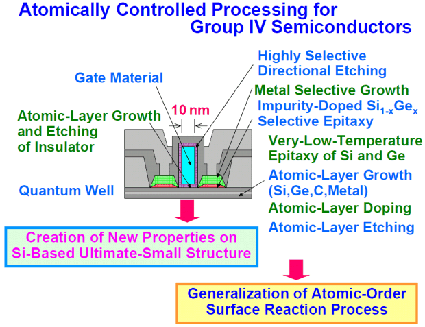
For highly functional semiconductor devices with ultrahigh speed and ultralow power for the Si LSIs, our atomically controlled processing technology by control of Langmuir-type adsorption and reaction in CVD (Chemical Vapor Deposition) becomes important increasingly. Utilizing the technology, we aim to create non-equilibrium strain-controlled Si-Ge-C group IV semiconductors with high carrier concentration and high carrier mobility by advancing atomically controlled heteroepitaxial growth of Si, Ge, SiGe, SiGeC and impurity (B, P, C, N and so on) to the extremity. Moreover, we also aim to establish a technological basis for highly controlled nanometer-order three-dimensional structure formation. In detail, the following researches are being advanced: (1) Control of extremely high carrier concentration due to non-equilibrium atomically controlled heteroepitaxial growth which utilizing thermal and plasma-enhanced reaction and so on at low temperatures, (2) Modulation of energy band structure and carrier mobility due to introduction of atomically controlled strain into Si and Ge, (3) Formation of the nanometer-order three-dimensional structure with subnanometer precision in in-plane direction by breaking the limit of lithography technology utilizing selective CVD epitaxial growth and selective etching with atomic layer control.
By the above researches, highly strained nanometer-order three-dimensional structures and room temperature resonant tunneling structures with higher performance which exceeds the limit of physical properties in use of existing Si, SiGe alloy and Ge materials will be created. Simultaneously, by applying them to device fabrication, creation of group IV semiconductor quantum-effect nanodevice applicable to the large scale integration will be expected.
Research topics:
1. Atomically controlled heteroepitaxial growth of Si-Ge-C group IV semiconductors
2. Atomic layer doping into nanometer-order heterostructures of group
IV semiconductors
3. Three-dimensional nanometer-order fabrication of group IV semiconductor
heterostructures
4. Control of properties in three-dimensional nanometer-order group IV
semiconductor heterostructures
5. Development of advanced CVD equipment for formation of three-dimensional
nanometer-order group IV semiconductor heterostructures
6. Fabrication process of Si-based nanometer-order heterostructure devices
|