9th
International WorkShop on
New Group IV
Semiconductor Nanoelectronics
and
JSPS Core-to-Core Program
Joint Seminar
"Atomically Controlled Processing for Ultralarge Scale
Integration"
Jan. 11(Mon.) - 12(Tue.), 2016
Conference Room (4th Floor)
Laboratory for Nanoelectronics and Spintronics
Research Institute of Electrical Communication
Tohoku University, Sendai, JAPAN
Cosponsored
by
ABSTRACT
DEADLINE : December 1, 2015
New! Time
Schedule
New! Program &
Abstracts
Registration
The 9th International
Workshop on New Group IV Semiconductor Nanoelectronics and JSPS
Core-to-Core Program Joint Seminar "Atomically Controlled Processing
for Ultralarge Scale Integration" will be held in Laboratory for
Nanoelectronics and Spintronics, Research Institute of Electrical
Communication, Tohoku University, Sendai, Japan, on January 11-12,
2016. This workshop will focus on new group IV semiconductor
nanoelectronics.
SCOPE
- Theoretical and Experimental Aspects
on Homo-and Heteroepitaxial growth
- Growth Mechanisms of Molecular Beam
Epitaxy and Chemical Vapor Deposition
- Formation and Properties of
Self-Organized/Quantum-Confined Structures
- Novel Growth Techniques
- Electronic and Crystallographic
Structures of Surfaces and Interfaces
- Si-Ge and Si-Ge-C and Other Group IV
Materials
- Silicides/Si(Ge, C) Heterostructures
- Oxides and Nitrides/Si(Ge, C)
Heterostructures
- Electronic Device Applications of
Si/Ge(C) Systems
- Optical Device Applications of
Si/Ge(C) Systems
- Si-Based Light Emission and Detection
- Relaxed Buffers, Compliant Substrates
- Doping in Group IV Systems
- Device Technology for Si-Based Group
IV Systems
SUBMISSION
OF ABSTRACTS
PDF
or MS Word file of Two-page
abstract (one-page main text and one-page figures), written
in English on white bond paper (A4 size; 2.5cm margin on four
sides), should be submitted by Dec. 1, 2015 to the Secretariat at the following
address:
| E-mail: |
 |
Secretariat of International WorkShop
on New Group IV Semiconductor Nanoelectronics,
Research Institute of Electrical Communication, Tohoku University
2-1-1, Katahira, Aoba-ku, Sendai,
980-8577, Japan
Tel.: +81-22-217-5548, Fax.:
+81-22-217-5551
All the
accepted abstracts will be expected to be
opened on this workshop web site. The abstract should be headed
by the title, author(s), affiliation(s), address, telephone
number, fax number and e-mail address, and clearly describe the
originality and new contributions of the work. The title,
author(s), affiliation(s), address, telephone number, fax number
and e-mail address should be also sent by E-mail to
Papers to
be presented at the workshop will be
selected by the Program Committee based on the submitted
abstracts. The notice of acceptance will be e-mailed to the first
author or corresponding author by Dec. 4, 2015.
.
INTERNATIONAL ADVISORY COMMITTEE
| M. Caymax (imec, Belgium) |
| S. Chiussi (Univ. Vigo, Spain) |
| J. Derrien (Aix-Marseille Univ., France) |
| J. L. Hoyt (MIT, USA) |
| E. A. Fitzgerald (MIT, USA) |
| E. Kasper (Univ. Stuttgart, Germany) |
| J. Murota (Tohoku Univ., Japan) |
| J. C. Sturm (Princeton Univ., USA) |
| V. Le Thanh (Aix-Marseille Univ., France) |
| B. Tillack (IHP & Tech. Inst. Berlin,
Germany) |
| S. Zaima (Nagoya Univ., Japan) |
ORGANIZING COMMITTEE
| M. Niwano (Chair, Tohoku Univ.) |
| J. Murota (Vice-Chair, Tohoku Univ.) |
| S. Sato (Tohoku Univ.) |
| T. Okumura (Tokyo Metropolitan Univ.) |
| M. Suemitsu (Tohoku Univ.) |
| M. Sakuraba (Tohoku Univ.) |
PROGRAM COMMITTEE
| J. Murota (Chair, Tohoku Univ.) |
| S. Zaima (Co-Chair, Nagoya Univ.) |
| S. Takagi (Univ. Tokyo) |
| S. Miyazaki (Nagoya Univ.) |
| K. Washio (Tohoku Univ.) |
| Y. Kunii (Hitachi Kokusai Electric) |
| J. Sakai (Canon Anelva) |
| A. Toriumi (Univ. Tokyo) |
| T. Tsuchiya (Shimane Univ.) |
| M. Miyao (Kyushu Univ.) |
| T. Ito (Osaka Univ.) |
WORKSHOP
PRESENTATIONS
Invited talk:
Each
talk will be scheduled as a presentation including
questions, comments, and discussions. Presentation time will be 30 min.
A PC projector will be available.
|
Regular
Oral talk:
Each
talk will be scheduled as a presentation including
questions, comments, and discussions. Presentation time will be 20 min.
A PC projector will be available.
|
Poster presentation and short oral talk:
Poster session will be scheduled. Each poster board is approximately
900 mm width and 1200 mm height, and will be labeled with the number of
the paper (e.g., P01).
Each
talk will be scheduled as a presentation NOT including
questions, comments, and discussions. Presentation time will be within 5 min.
A PC projector will be available.
|
TIME SCHEDULE &
PROGRAM
New! Time
Schedule
New! Program &
Abstracts
REGISTRATION
The
Workshop registration desk will be open tentatively for
09:00-17:00 on Monday, Jan. 11, 2016.
09:00-17:00 on Tuesday, Jan. 12, 2016.
| |
Registration Fee
|
Banquet Fee
|
|
Regular
|
0 JPY
|
4,000 JPY
|
|
Student
|
0 JPY
|
Attendees are recommended to send completed registration
form to Secretariat (e-mail or fax) in advance. Payment for banquet must be made in Japanese yen by
cash at registration desk. (Credit cards, personal checks and
bank checks are NOT ACCEPTABLE.)
BANQUET
A banquet will be
held at 18:00-20:00 on Monday, Jan. 11, 2016 at Hotel Bel Air Sendai (1st Floor).
CORRESPONDENCE
For
further information, please contact to:
Secretariat of
International WorkShop on New Group IV Semiconductor Nanoelectronics,
Research Institute of Electrical Communication
Tohoku University
2-1-1, Katahira, Aoba-ku, Sendai, 980-8577, Japan
Tel: +81-22-217-5548, Fax: +81-22-217-5551 |
|
E-mail:
|
|
|
| |
TRANSPORTATION
Sendai
Sendai is located 350
kilometers north of Tokyo on the pacific coast of Japan. Domestic
flights to Sendai from Nagoya airports are available. The JR
Shinkansen Express (bullet train) connects major cities in Japan,
and it takes only 2 hours from Tokyo to Sendai. The trip from
Narita Airport to Sendai takes around 3.5 hours by Narita Express
(a shuttle between the airport and Tokyo) or Keisei Line (a
railway between the airport and Ueno) and Shinkansen. Sendai
International Airport also services seven international
destinations. From Sendai International Airport to JR Sendai
Station, a new railway (Sendai Airport Access Line) and a
conventional public shuttle bus run frequently.
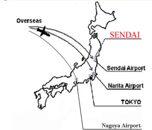
Via New Tokyo International Airport
(Narita)
Participants arriving in New
Tokyo International Airport (Narita Airport) have the following
options for traveling to Sendai via Tokyo. Take either the JR Narita Express Train
or a Limousine Bus to Tokyo Station. Narita Express is available
at 30 minutes interval and it takes approximately 60 minutes from
Narita to Tokyo Station at about 3000 yen. Limousine Bus is
available every 15 minutes and it takes 80 minutes at about 3000
yen. Take the JR Shinkansen Express (bullet train) from Tokyo
Station to Sendai. The train is available every 15 minutes and it
takes 2 hours at about 11,000 yen. For more details, visit the JR
East website: http://www.jreast.co.jp/e/index.html
Via Sendai International Airport
Railway
(Sendai Airport Access Line)
is available to JR Sendai Station at 630 yen.
Scheduled travel time: 25 minutes.
From JR Sendai Station
-->
Sendai City Map (1 Mbytes)
From JR Sendai station to Laboratory
for Nanoelectronics and Spintronics,
Research Institute of Electrical Communication, Tohoku Univ., it
takes approximately 15 minutes on foot.
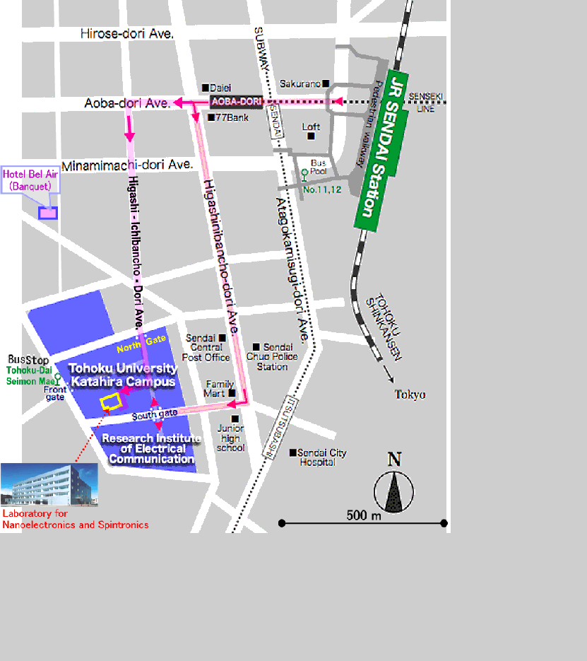
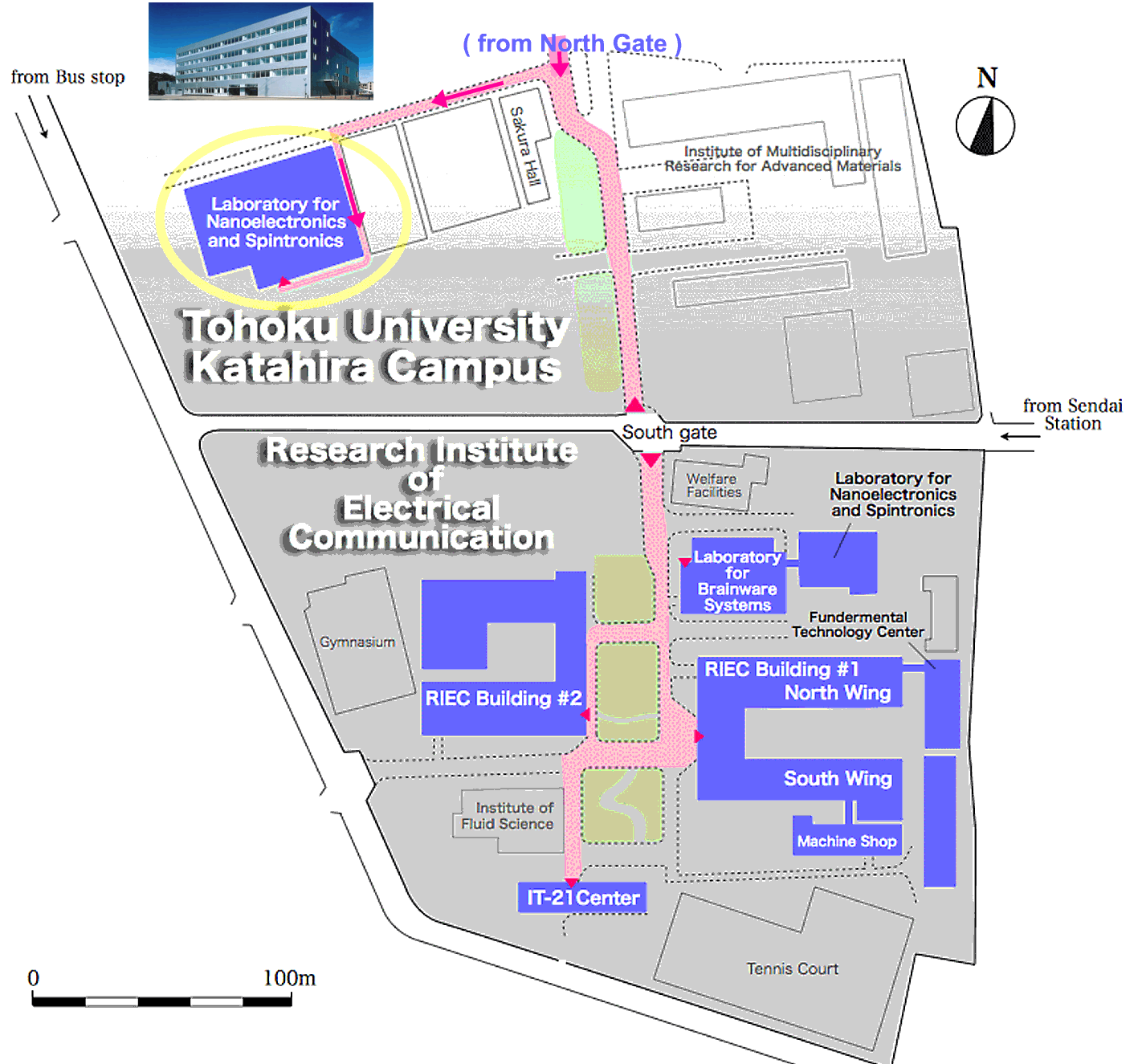
Download
Map.doc (260 kbytes)
LINK
Research Institute of
Electrical Communication (RIEC), Tohoku University
Japan
Society for the Promotion of Science (JSPS) Core-to-Core Program
"Atomically Controlled Processing for Ultralarge Scale
Integration"